
Metal additive manufacturing (AM) company Sintavia has installed a Nikon Metrology computed tomography (CT) system at its facility in Florida, US to help control the AM process.
Using powder-bed AM with electron and laser-beam melting, Sintavia currently manufactures components from Inconel 718 and 625, aluminium, titanium, cobalt-chrome, stainless steel and other proprietary powders.
AM allows special internal designs to be realised, such as conformal cooling channels, lattice networks, hollow members and other complex geometries. Both additive and traditional manufacturing can result in microscopic voids and gaps within the structure, which can cause stress fractures and reduce the longevity of a component’s lifecycle. All of these internal features can only be inspected non-destructively with CT scanning.
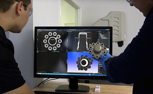
Sintavia has installed a 450 kVA micro-focus CT (micro-CT) system from Nikon Metrology. By converting 2D pixels to 3D voxels, supplying a full 3D density map of the samples, the technique presents information in a visual, easy-to-interpret format and shows any departure from the CAD model. It is said to be straightforward to detect and measure powder residues blocking channels, porosity, contamination, cracking, warping, and dimensions such as wall thickness to an accuracy within tens of microns. Given a 100 mm sample and a detector 2000 pixels across, the limiting resolution would be 50 µm, for example.
Micro CT is now much faster and more suitable for production-line use, while CT scanning of similar parts can be automated using loading and unloading equipment. Scan times down to a few tens of seconds per part are possible.
For further information www.nikonmetrology.com